إنتل 80486
المعالج أنتل 80486 والمعروف أيضا بـ i486 أو 80486 (بالإنجليزية: Intel 80486) وهو معالج ذو أداء عالي وتبع المعالج إنتل 80386
| Intel 486 وحدة المعالجة المركزية | |
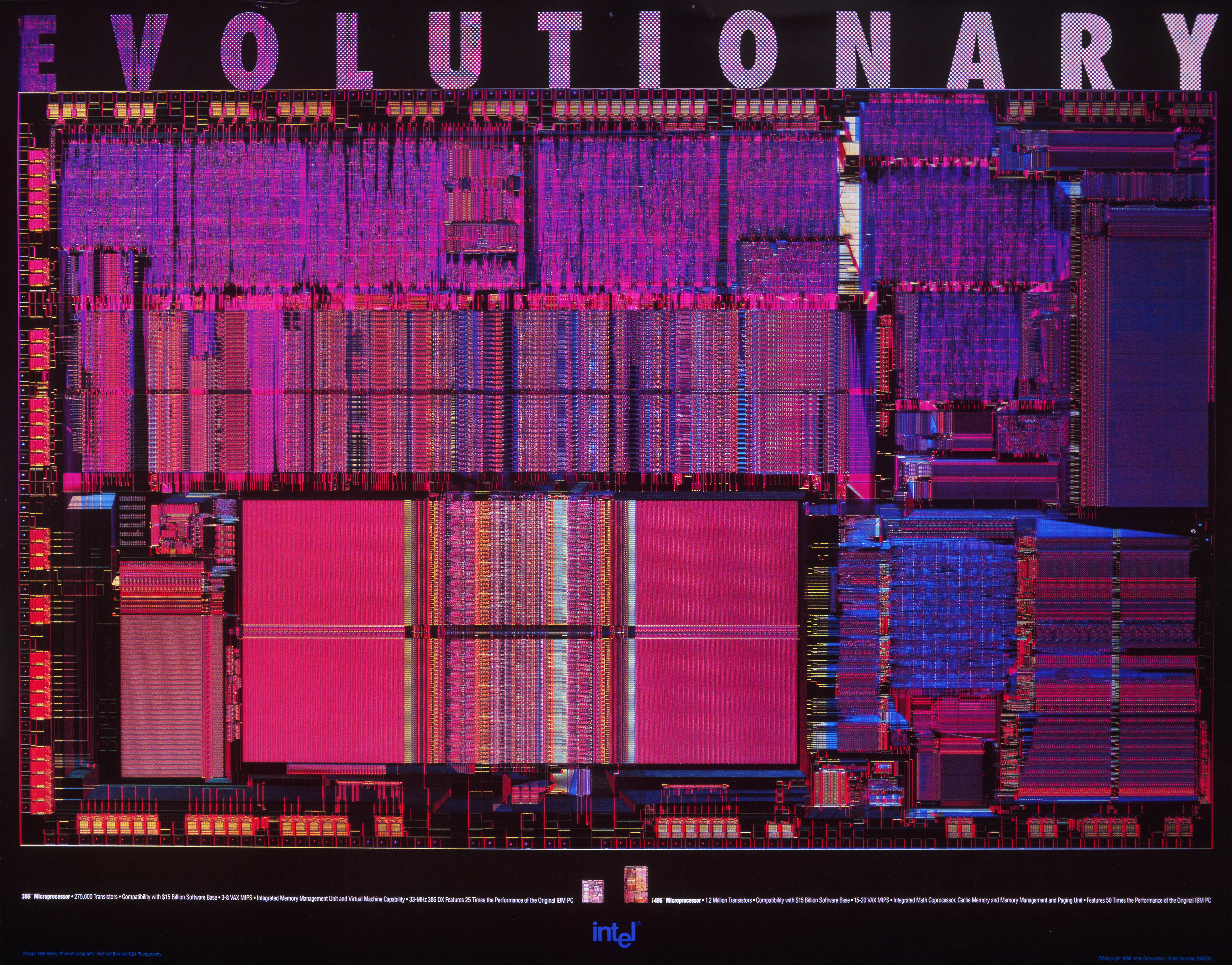
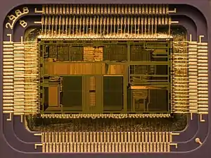 الجزء المعرض للخطر من (يسمى die) أي معالج 80486DX2 | |
| أُنتج: | 1989 |
| أصغر حجم: | 1 µm إلى 0.6 µm |
نبذة تاريخية
أعلن عنه (486) في ربيع المعرض الدولي السانوي كومديكس في أبريل 1989 عندما أعلنت إنتل
تحسينات
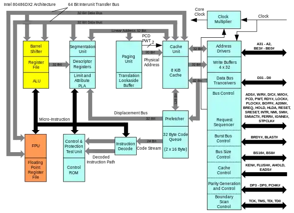
The 486DX2 architecture
| Intel 486 registers | ||||||||||||||||||||||||||||||||||||||||||||||||||||||||||||||||||||||||||||||||||||||||||||||||||||||||||||||||||||||||||||||||||||||||||||||||||||||||||||||||
| ||||||||||||||||||||||||||||||||||||||||||||||||||||||||||||||||||||||||||||||||||||||||||||||||||||||||||||||||||||||||||||||||||||||||||||||||||||||||||||||||
| ||||||||||||||||||||||||||||||||||||||||||||||||||||||||||||||||||||||||||||||||||||||||||||||||||||||||||||||||||||||||||||||||||||||||||||||||||||||||||||||||
| ||||||||||||||||||||||||||||||||||||||||||||||||||||||||||||||||||||||||||||||||||||||||||||||||||||||||||||||||||||||||||||||||||||||||||||||||||||||||||||||||
| نموذج أو موديل | السرعة القصوى clock | الفولت (Voltage) | ذاكرة مخبئية | ظهر في | ملاحظات | |
|---|---|---|---|---|---|---|
  | i486DX (P4) | 20, 25 MHz 33 MHz 50 MHz | 5V | 8 KB WT | April 1989 May 1990 June 1991 | The original chip (without any clock doubling) |
 | i486SL | 20, 25, 33 MHz | 5V or 3.3V | 8 KB WT | November 1992 | Low power version of the i486DX, reduced VCore, SMM (System Management Mode), stop clock, and power saving features – mainly for use in portable computers |
 | i486SX (P23) | 16, 20, 25 MHz 33 MHz | 5V | 8 KB WT | September 1991 September 1992 | An i486DX with the FPU part disabled or missing. Early variants were parts with disabled (defective) FPUs.[1] Later versions had the FPU removed from the die to reduce area and hence cost. |
 | i486DX2 (P24) | 40/20, 50/25 MHz 66/33 MHz | 5V | 8 KB WT | March 1992 August 1992 | The internal processor clock runs at twice the معدل ساعة (حاسوب) of the external bus clock |
| i486DX-S (P4S) | 33 MHz; 50 MHz | 5V or 3.3V | 8 KB WT | June 1993 | SL Enhanced 486DX | |
 | i486DX2-S (P24S) | 40/20, 50/25 MHz (66/33 MHz) | 5V or 3.3V | 8 KB WT | June 1993 | |
 | i486SX-S (P23S) | 25, 33 MHz | 5V or 3.3V | 8 KB WT | June 1993 | SL Enhanced 486SX |
 | i486SX2 | 50/25, 66/33 MHz | 5V | 8 KB WT | March 1994 | i486DX2 with the FPU disabled |
 | IntelDX4 (P24C) | 75/25, 100/33 MHz | 3.3V | 16 KB WT | March 1994 | Designed to run at triple clock rate (not quadruple as often believed; the DX3, which was meant to run at 2.5× the clock speed, was never released). DX4 models that featured write-back cache were identified by an "&EW" laser etched into their top surface, while the write-through models were identified by "&E". |
 | IntelDX4WB | 100/33 MHz | 3.3V | 16 KB WB | October 1994 | |
| i486DX2WB (P24D) | 50/25, 66/33 MHz | 5V | 8 KB WB | October 1994 | ||
| i486DX2 (P24LM) | 90/30 MHz; 100/33 MHz | 2.5–2.9V | 8 KB WT | 1994 | ||
 | i486GX | up to 33 MHz | 3.3V | 8 KB WT | Embedded Ultra-Low power CPU with all features of the i486SX and 16 bit external data bus. This CPU is for embedded battery-operated and hand-held applications. |
روابط خارجية
انظر أيضا
مراجع
- Newnes 8086 Family Pocket Book – Ian Sinclair (ISBN 0 4349 1872 5)
 بوابة كهرباء
 بوابة إلكترونيات
 بوابة تقنية المعلومات
 بوابة علم الحاسوب
في كومنز صور وملفات عن: إنتل 80486
This article is issued from Wikipedia. The text is licensed under Creative Commons - Attribution - Sharealike. Additional terms may apply for the media files.